Electronics by Manmohan Pal: February 2018

Tuesday, February 6, 2018

LED CHASER

LED Chaser

LED chaser circuit using IC 555 Timer and 4017 Decade counter by Manmohan Pal


Sequential running LED lights 


Using IC 555 Timer and IC CD 4017


LED Chaser circuits using IC 4017 + IC 555


If you want to build a 10 LED Chaser circuit we suggest this circuit first. It uses popular IC is a simple and affordable IC-4017_decade counter and IC-555.


As circuit diagram below is LED chaser circuit which The CD4017 act as LED driver in 10 output, by LED will glow only one in a rapid sequence. And control to speed with VR1 which is setting frequency output of a basic astable or free-running pulse generator with IC-555 as main.


10 LED Chaser Circuit


This is the circle 10 LED running light as another kind of string light circuit. Which is running light on circle each one step beautifully and can adjust speed as well.
The working principle
From circuit will see that we use two ICs. Which is IC1-NE555 as timer IC with a widely used general. In this circuit will use the IC-555 as the square wave generator to output. Which that frequency is determined by R-2.7K, R-470 ohms and C-10uF 16V.


In addition yet has a VR1-potentiometer-10K is frequency adjuster. When IC1-NE555 generate the frequency up, will be entered to IC2-CD4017 by through way of R 100 ohms. IC2 is Decade Counter IC will provide output is positive voltage Sort by Position according to input signal from IC1-NE555 One end of the LED all. Which is pin K to pooling through R 1K to ground to as the through way of current.

Youtube link for easy LED chaser circuit

https://www.youtube.com/watch?v=Ohuu0gyTOBU


How to assemble circuits
You can build the PCB as layout in Figure 2. Then Put all parts in PCB as components layout in Figure 3. Firstly, put small components type such as R, C, LED and socket IC in to PCB. When solder finish, should check correctly. Next bring both IC insert in to socket, careful do not Wrong terminal. When check all thing correct then enter power supply into the circuit. Then, adjust trimmer potentiometer and noticed the running of LED if all what work normally so can use it now.


The components List.


1. IC-CD4017  Decade Counter IC -                  1 pcs.
2. IC-NE555 Timer IC-                                      1 pcs.
3. C-10uF 16V- Electrolytic capacitors-             2 pcs.
4. R-2.7K- Resistors- 1/4 W 5%-                        1 pcs.
5. R-470 ohms- Resistors- 1/4 W 5%-                1 pcs.
6. R_1K Resistors- 1/4 W 5%-                            1 pcs.
7. VR_10K__trimer-potentiometer- _                 1 pcs.
8. LED (any colour )                                        10 pcs.


Please refer more videos and interesting videos


Please subscribe my Youtube channel

https://www.youtube.com/user/mannmohanpal

Manmohan Pal
Whatapp 8989811397
mannmohanpal@gmail.com

Blog:
http://electronics4ubymanmohanpal.blogspot.in/p/blog-page_2.html https://manmohanpal.wordpress.com/led-blinking-circuit/


Twitter: 
@ManmohanPal15

Facebook Page:
https://www.facebook.com/mannmohan.pal.7
https://www.facebook.com/Electronics-by-Manmohan-Pal-1802344069857656/?view_public_for=1802344069857656

Monday, February 5, 2018

LDR Circuit : Automatic Street Light

 Automatic Street Light
Science Project
Simpal LDR Circuit using IC 555 Timer: Automatic Street Light DIY by Manmohan Pal


Here we have explained a dark detector circuit by using 555 timer IC and a LDR (Light Dependent Resistor) which senses the light in surroundings and if it does not find the light, it triggers the IC and glows an LED attached with the circuit. In place of LED we can also use a buzzer or speaker to use it as dark detector alarm. The concept of this LDR circuit is quite simple and based on the working of LDR. So lets first understand more about LDRs.


Video link : LDR circuit using IC 555 Timer

https://www.youtube.com/watch?v=1gwUOnkJzxY


LDRs are a type resistors made from semiconductor materials to enable them to have their light sensitive properties. There are many types of LDRs but one of the most popular material used is cadmium sulphide (CdS). These LDRs or also known as photo resistors works on the principle of “Photo Conductivity”. Now what this principle says is , whenever light falls on the surface of the LDR (in this case) the conductance of the element increases or in other words the resistance of the LDR falls when the light falls on the surface of the LDR. This property of the decrease in resistance for the LDR is achieved because it is a property of semiconductor material used on the surface.


Here in this dark detecting LED circuit, LDR is configured with 555 timer IC in ASTABLE mode in such a way that 555 ASTABLE generates square wave when the light intensity goes below a certain level.


1. pin no 6 is connected to pin no 2
2. pin no 4 is connected to pin no 8
3. a resistor of 5 k is connected between pin no 1 and pin no 2
4. a LDR is placed between pin no 4 and pin no 2
5. LED is connected between pin no 1 and pin no 3


When there is dark on LDR the LEDs are ON  i.e. at night lights will glow automatically
Where there is light on LDR the LEDs are off  i.e. in day time lights are off automatically


above figure shows the circuit diagram of dark detecting LED. This circuit shows how we can convert a simple astable mode circuit to a “dark sensor”. We just need to add an LDR and a resistor in the circuit, then it simply works as dark detector. A general purpose LDR is used for sensing the light. When proper light is falling on the LDR its resistance is very low. When there is no light the LDR resistance increases. At this time the IC is triggered and glows the LED attached with the circuit


Manmohan Pal
Mob. 8989811397
Email- mannmohanpal@gmail.com
Youtube Channel: https://www.youtube.com/channel/UCDnhARnHOEIPuNIEp5vPdGQ

Automatic Street Light Circuit


Sunday, February 4, 2018

Logic Gates

AND Gate


Logic AND Gate Tutorial

A Logic AND Gate is a type of digital logic gate that has an output which is normally at logic level “0” and only goes “HIGH” to a logic level “1” when ALL of its inputs are at logic level “1”.

The output state of a “Logic AND Gate” only returns “LOW” again when ANY of its inputs are at a logic level “0”. In other words for a logic AND gate, any LOW input will give a LOW output.
The logic or Boolean expression given for a digital logic AND gate is that for Logical Multiplication which is denoted by a single dot or full stop symbol, ( . ) giving us the Boolean expression of:  A.B = Q.
Then we can define the operation of a 2-input logic AND gate as being:


Symbol Truth Table
2-input AND gate
2-input AND Gate
B A Q
0 0 0
0 1 0
1 0 0
1 1 1
Boolean Expression Q = A.B Read as A AND B gives Q           

 
Follow the link to make And gate demonstration science project 


7408 Quad 2-input AND Gate

7408 logic and gate
In the next tutorial about Digital Logic Gates, we will look at the digital logic OR Gate function as used in both TTL and CMOS logic circuits as well as its Boolean Algebra definition and truth tables.


Friday, February 2, 2018

IC NE 555 Timer


IC NE 555 Timer


555 timer IC is the cheap, popular and precise timing device used in various applications. It gets the name from the three 5KΩ resistors that are used to generate two comparator reference voltages. This IC is operated as monostable, bistable or astable multivibrater to produce a variety of applications.


This IC comes with bipolar 8 pins dual in-line package. It consists of 25 transistors, 2 diodes and 16 resistors arranged to form two comparators, flip-flops, and high current output stage.


Pin Description

The following is the Pin Description

Pin 1-Ground: It is connected to ground as usual. For the timer to function this pin should be connected to ground.

Pin 2-TRIGGER: The negative input comparator No 1. A negative pulse on this pin “sets” the internal Flip-flop when the voltage drops below 1/3Vcc causing the output to switch from a “LOW” to a “HIGH” state
Pin 3-OUTPUT: This pin also has no special function. This pin is drawn from PUSH-PULL configuration formed by transistors.This pin gives the output.
Pin 4-Reset: There is a flip-flop in the 555 IC timer chip. The output of flip-flop controls the chip output at pin 3 directly. This pin is connected to Vcc for the flip-flop to stop from hard resetting.
Pin 5-Control Pin: The control pin is connected from the negative input pin of comparator one. The function of this pin to give the user the direct control over the first comparator.
Pin 6-THRESHOLD: Threshold pin voltage determines when to reset the flip-flop in the timer. The threshold pin is drawn from positive input of comparator1.
Pin 7-DISCHARGE: The discharge pin is connected directly to the Collector of an internal NPN transistor which is used to “discharge” the timing capacitor to ground when the output at pin 3 switches “LOW”.
Pin 8-Power or VCC: This pin also has no special function. It is connected to a positive voltage.
Working Modes OF 555 Timer IC


The 555 timer IC operates in modes

Astable mode


Monostable mode


Bistable mode

Astable mode
Astable mode means there will be no stable levels at the output. Thus the output will fluctuate from high and low. This character of the astable output is used as a clock or square wave output for many applications.

Features of 555 timer IC
It operates from a wide range of power supplies ranging from + 5 Volts to + 18 Volts supply voltage.
Sinking or sourcing 200 mA of load current.
The external components should be selected properly so that the timing intervals can be done in several minutes along with the frequencies exceeding several hundred kiloHertz.
The output of a 555 timer can drive a transistor-transistor logic (TTL) due to its high current output.
It has a temperature stability of 50 parts per million (ppm) per degree Celsius change in temperature, or equivalently 0.005 %/ °C.
The duty cycle of the timer is adjustable.
The maximum power dissipation per package is 600 mW and its trigger and reset inputs has logic compatibility.
Thus, this is all about making of Blinking LED using a 555 timer IC. We hope that you have got a better understanding of this concept. Furthermore, any queries regarding this topic or 555 timer based projects, please give your valuable suggestions by commenting on the comment section below.


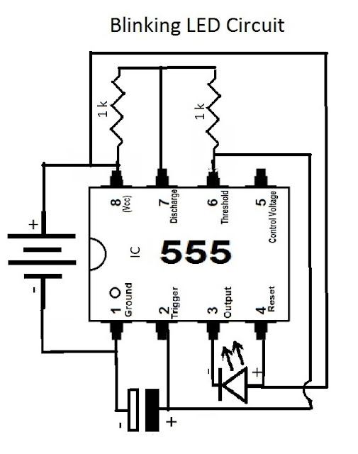
Simple Blinking LED

Simple blinking LED circuit

LED blinking Circuit


Blinking LED Circuit Using a 555 Timer IC

Circuit Components
1. 555 timer IC
2. LED
3. 3.7 V mobile phone battery
4. 1KΩ Resistor – 2
5. 100µF Capacitor
6. Bread Board
7. Connecting wires

Circuit Diagram
The following circuit design explains the design of the blinking LED with the 555 timer IC. Here in this configuration, the 555 timer IC has connected in an Astable mode of 555 timer operation.


  • Collect all the required components and place the 555 timer IC on the breadboard.
  • Connect pin 1 of a 555 timer IC to the ground. You can find the pin structure of a 555 timer IC in the circuit diagram shown above.
  • The longer lead of a polarized capacitor is the positive and the shorter lead is negative. Connect pin 2 to the positive end of a capacitor. Connect the negative lead of the capacitor to the ground of the battery.
  • Now short the pin 2 to pin 6 of the 555 timer IC.
  • Connect the output pin 3 with the positive lead of the LED using a 1kΩ resistor. The negative lead of LED needs to be connected with the ground.
  • Connect pin 4 to the positive end of the battery.
  • Pin 5 does not connect to anything.
  • Connect pin 6 to pin 7 using a 470kΩ resistor.
  • Connect pin 7 to the positive end of the battery using a 1kΩ resistor.
  • Connect pin 8 to the positive end of the battery
Finally, connect the battery leads with the breadboard to start the power supply in the circuit.


By: Manmohan Pal
Email: mannmohanpal@gmail.com
Whatsapp: 8989811397
Blog: http://electronics4ubymanmohanpal.blogspot.in/

http://electronics4ubymanmohanpal.blogspot.in/p/blog-page_2.html
https://manmohanpal.wordpress.com/led-blinking-circuit/

Youtube Channel:  https://www.youtube.com/channel/UCDnhARnHOEIPuNIEp5vPdGQ